


For IGBT, no conducting channel will be formed with no voltage on G and, the resistance of C-E is particularly high . Therefore, digital multimeter “×10KΩ”gear, show the value similar to "∞". In theory, C-E resisitance equals to a positive PN junction resistance and a reverse PN junction resistance. I The E-C resistance of GBT is 55kQ and C-E resistance RCE ≥ 107 Ω.
Diode measurements of IGBT
As the insulated gate bipolar transistor and diode package are usually packaged together and made into modules, red test pen should be connected to “E” electrode, and the black one to “C” electrode. diode forward voltage should drop around 0.4V voltage (for some without built-in diode model, such as GT40T101, there is no voltage drop).
For IGBT, no conducting channel will be formed with no voltage on G and the resistance of C-E is particularly high . Therefore,C-E is off when using digital multimeter device file diode.and E-C diode profile measurement for the freewheeling diode forward voltage drop 0.3V.
1. The use of IGBT
(1) The design of driving protection circuit
The design of driving circuit is the key to decide whether IGBT can give full play to its performance.
Protection circuit is the important measures to protect IGBT from damages in overcurrent, overvoltage and other abnormal conditions, We must design it based on the .understanding of device characteristics and combined with device characteristics.
(2) junction temperature thermal design
Each IGBT has the maximum allowable junction temperature Tj. We need to control GBT’s Tj within its maximum value when it is working In general, IGBT cannot work without radiators. Radiators should be designed according to the loss of the device so as to ensure that the Tj junction temperature does not exceed the allowable value.
First of all, we need to calculate the loss of IGBT in the circuit. It contains two parts: one is the loss of the IGBT internal transistor, the other is the loss of the IGBT anti-parallel diode.
Loss of the IGBT internal transistor includes IGBT’s conduction and switching losses (switching losses includ turn-on loss and turn-off losses, which could be zero in soft switch circuit). The loss of diode includes diode conduction losses and diode recovery loss. The total loss can be obtained by adding all of losses up. The design should be conducted in accordance with the maximum loss, the maximum junction temperature IGBT at work can be obtained by the following heat equation
Tj =P∑{Rthjc+Rthcs+Rthsa} +Ta
In the formula, P∑ is the maximum power loss of IGBT; Rthjc is the thermal resistance from IGBT node to shell; Rthcs is the thermal resistance from the radiator to shell; Rthsa reprents heat resistance from radiator to the ambient space; Ta stands for the outside temperature. According to the above formula, Tj junction temperature can be obtained and therefore helps us to select suitable radiator..
(3) Connect in parallel
When IGBT module is used to control large current, sometimes devices are used in parallel. In the design, it is important to make sure that equal amount of current pass devices in parallel . Once the current lose balance, then one of devices may be damaged due to the concentration of current.
(4) custody and rules
The most appropriate storage places of power electronic equipment is 5 ~ 35 ℃ with humidity of 45% ~ 75%. IGBT and power transistors, in particular, need humidifying by humidifier if they are placed in a very dry area,. Furthermore, the chlorine contained in tap water will rust the wire of electronic, so we need to use pure water or distilled water and avoid places with corrosive gas and dust.
At places with rapid temperature changes, surface of power electronic equipment tend to have condensation. Therefore, these places should be avoided.
Semiconductor electronic devices should be put in containers that are not easy to generate static electricity.
(5) Others
The driving voltage can be measured in the terminal part (UCE), and there may be deviation between the applied voltage to driving circuit and the actual effect in the IGBT.. Pulse voltage is measured at the terminal part of the product.
Products must be used in the absolute maximum rated value (temperature, voltage, current, etc.) range. Once beyond the absolute maximum ratings, devices may be damaged.
IGBT should be used within the power cycle life.
When reverse gate voltage -UGE is insufficient, false triggering may occur. In order to prevent it, sufficient UGE value should be set (Recommended -15V).
If du/dt is high, false triggering may occur to bias circuit IGBT. In order to prevent false triggering, it should be used in the most appropraite gate trigger drive (+UGE、-UGE., RG).
2. IGBT’s protection circuit
When power electronic circuit is working, due to external error or misoperation, , protection circuit should be designed in the power electronic circuit in order to ensure the safety of electrical equipment and users and at the same time minimize the losscaused by abnormal operation. Widely-used protection circuit of IGBT has two types: the overcurrent protection and overvoltage protection.
2.1 Overcurrent protection
The overcurrent of IGBT is often caused by short circuit. When the short circuit occurs, IGBT collector current will increase rapidly and exceeds the rated value, which causes a rise in the UCF voltage of IGBT Collector - emitter and then IGBT power loss increase. It it exposed to this condition for a long time, IGBT’s junction temperature will exceed the allowable value and at last be burned.
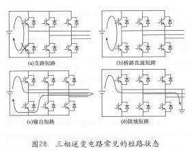
Causes of short circuit may have many kinds. Next let’s take a three-phase inverter circuit as an example to introduces the common short circuit state:
(1) Branch short-circuit
short circuit caused by GBT or its anti parallel diode, see Figure 28 (a).
(2) Bridge short-circuit
Switching fault caused by control circuit, driving circuit or interference led to two IGBT at one bridge arm conduct at the same time, see Figure 28 (B).
(3) Output short circuit
Short circuit caused by assembly errors or load insulation damage,see Figure 28 (c).
(4) Grounded short circuit
Grounded short circuit caused by,human error, like wire distribution, see Figure 28 (D).
2.2 Over current protection method
In order to achieve over-current protection, it is imperative to test overcurrent status. For IGBT, there are two kinds of overcurrent detection methods:
current sensor test method and saturation voltage drop test of IGBT
(1) Current sensor test
By adding a current sensor in the circuit, we can test the current in the circuit, and then then judge whether the IGBT is overcurrent. This method can detect and distinguish all kinds of short circuit , so as to take different protection strategies respectively to reduce the loss caused by the abnormal circuit.
In addition, if the current of IGBT is turned off too fast, overvoltage will occur between the collector and emitter, causing IGBT damage. Therefore, after overcurrent has been detected, certain measures should be taken to turn the IGBT off and make the turn-off process take place in reverse bias safe operating area (RBSOA), that is to say the so-called "soft shut" should be adopted.
(2) IGBT saturation voltage drop test
When overcurrent occurs, the saturation voltage drop UCE(sat) of IGBT is higher than normal condition.
Figure 29 is an over-current protection circuit using the indirect voltage method. it can detect the overcurrent of IGBT by adopting the principle that the value of UCE will increase when overcurrent occurs,. .The internal circuit of M57959AL drive can successfully complete soft shut. UCE containing current information can fastly recover the test of diode VD2, and then directly transmits to the M57959AL’s collector voltage monitoring terminal 1, pin 8 output; It will then be sent to reference voltage of comparator U1A’s positive end and reverse side through the U2 photoelectric coupler. After comparison, ouput is made and drive signal can be turned off. If over-current emerges, drive M57959AL will slowly cut off IGBT, to avoid damages caused by r voltage spike due to large di/dt , and reduce the noise level.
At present, similar protection circuit is built in within most GBT’s special driving chip

There are several ways to inhibit IGBT from turning-off surge voltage are as follows:
(1) Installation of the buffer circuit in IGBT and using film capacitor that can absorb high-frequency voltage surge;
(2) Adjust the turn-off bias voltage -UCE and the gate drive resistance RG in IGBT driving circuit to reduce the turn-off di/dt;
(3) Reduce the lead inductance of the main circuit and snubber circuit, use wire as thick and short as possible; in addition, using flat wiring (hierarchical wiring) can effectively reduce the lead inductance. The buffer circuit of IGBT has two kinds of configuration methods: one is configured for each IGBT buffer circuit individually; another is the installation of a centralized buffer circuit for multiple IGBT. Separately configured buffer circuits that are commonly used include RC buffer circuit, charge and discharge type RC-VD buffer circuit and the discharge stop type RC-VD buffer circuit.
RC buffer circuit can be seen in figure 30. Between the collector and emitter of the IGBT a RC series branch is in parallel, which can be applied to the chopper circuit. But RC series branch will discharge through IGBT when IGBT is opened, which leads to a current increase of IGBT when it is turned on and additional IGBT load; in addition, in RC buffer circuit, every time, after turn-off, electric energy stored in the capacitor will be consumed in the form of heat. Since its loss is bigger, it is not suitable to be adopted frequently.. The Loss of RC buffer is
![]()
In the formula: Csunber is buffer circuit capacitance; Ud represents forward voltage drop when IGBT stop ; fs stands for switching frequency.

Comparison of the charge and discharge type RC-VD buffer circuit and RC buffer circuit, adds a resistance and a diode connected in parallel, see figure 31. Through the diode capacitance branch, improve the ability to inhibit surge voltage buffer circuit shut off. Join the diode, increasing the buffer resistance, reduce current carrying on IGBT in the opening. But compared with the discharge stop type RC-VD buffer circuit, the loss is great. Loss of charge and discharge type RC-VD buffer circuit is
![]()
In the formula: L is main circuit inductance; Ic stands for collector current when IGBT is off; Cs represents buffer capacity; Ud is DC voltage; fs is switching frequency.
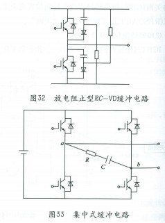
Buffer circuit structure of the discharge stop type RC-VD can be seen figure 32. It’s suitable to absorb two IGBT voltage surge on one bridge arm . It can effectively eliminate the surge voltage when the IGBT is switched off, and the loss of the buffer circuit is less than the previous two kinds of buffer circuit and is suitable to be used frequently. Its loss can be calculated as follows
![]()
In the formula: L is main circuit inductance; Ic stands for collector current off for IGBT; fs is switching frequency.
Centralized buffer circuit is suitable when a plurality of IGBT is used simultaneously ,just like figure 33. In this diagram, through the parallel a RC circuit at two output terminals of a full bridge inverter, the voltage can be absorbed when the four IGBT is turned off.